


AMD 3D V-Cache, meet the 3D design that increases the FPS in Ryzen
At Financial Analyst Day, AMD revealed that it was working on 3D stacking technologies, such as X3D. Back in May, they showed the impact of 3D V-Cache in video games, but that is not the only goal of AMD: it will start with EPYC Milan-X and then it will reach Zen 4 processors .
The roadmap is already defined and the first processors to incorporate 3D V-Cache technology will be the EPYC Milan-X, a subfamily of Milan, which are based on the Zen 3 architecture. of bandwidth for the processor, whose consequences are tremendous for companies and gamers, we explain it to you!
Index of contents
Timeline: how X3D packaging starts
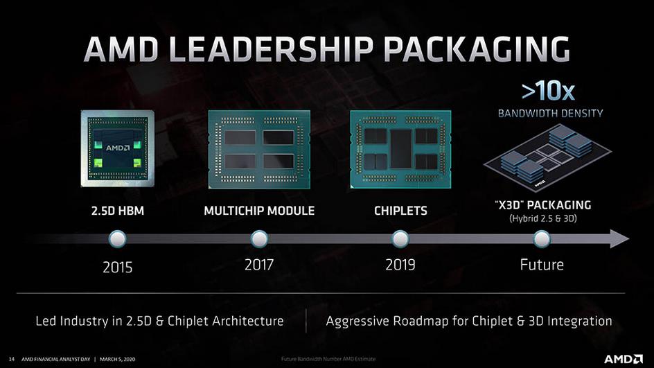
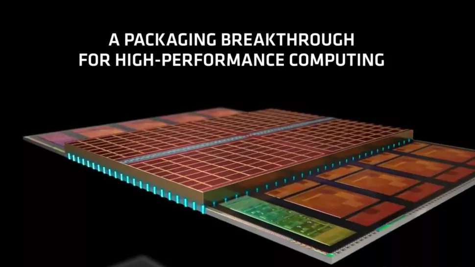
It all starts in March 2020, at which point AMD announces its research on 3D stacking technologies, appearing ” X3D packaging “. This is what we saw in the slide that showed where the designs adopted by AMD itself during the last 5 years were seen. The future aimed to design processors with 3D packaging, whose complexity is evident and is a task that remains in the hands of TSMC (in this case).
AMD claimed that it was a fusion of 2.5D and 3D packaging technologies , capable of offering a bandwidth up to 10 times higher than the current one. Hence we see the word ” hybrid ” (hybrid), but the funny thing is what happens from this moment: TMSC announces its 3D Fabric technologies , preparing to receive orders for chips with 3D design.

The presentation of AMD Ryzen 5000 and the Zen 3 architecture on the desktop arrives , an event in which Lisa Su shows a chip (which was a prototype) characterized by having a dual chiplet : in one we have a 64 MB SRAM. This is a breakthrough in cache memory , and it is now that the CPU cores could simultaneously access the L3 cache.
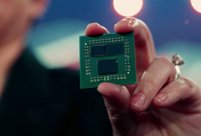
We saw how an 8-core Die could access 96 MB L3, instead of 32 MB. If you look closely, the chip has the 2 DIEs attached, and for this they use a TSV (Throught Silicon Vias), which allows the passage of energy and data between them; what becomes a lifelong bridge. In this way, the bandwidth of the L3 cache could go beyond 2 TB / s, which is insane.
And the TSV is a die <-> die copper direct interconnect interface, so all eyes are on Chip-on-Wafer (CoWoS), a TSMC technology that AMD would be using for it.
The core complex and the cache die have different sizes, so the solution is to use additional silicon in order to maintain the same pressure over the 2 dies. You will see that the 2 dies are finer than the other complex.
Lisa Su explained that all chiplets would cache stacked, namely 96 MB / chiplet , which would be 192 MB for a chip over 8 cores, ¿Ryzen 9? Threadripper? The key is that this 3D design allows:
- Interconnect density multiplied by 200 or more, compared to 2D.
- Triple the efficiency of the interconnection.
What is 3D V-Cache and why it matters
3D V-Cache technology is a 3D chiplet design by which L3 cache memory is stacked one on top of another, interconnecting them through a TSV to increase its bandwidth , as well as its capacity. In this way, the processor would improve its bandwidth, but, in addition, it would be able to equip much more L3 cache memory.
The V-Cache sits on top of the main CCX’s L3 cache , so no temperature issues are expected from it. Although memory is stacked on top of each other, processors with this technology are the same height as Zen 3 chips, but how is it possible? AMD achieves this by thinning the central chiplet and the V-Cache in order to have the same height as the die IOD. Mind you, the 3D V-Cache die is denser than normal L3 memory.

In the Ryzen 5000 we saw up to 64 MB of cache memory, but thanks to 3D V-Cache we can see processors with 192 MB and even more. The first chips with 3D V-Cache technology are the EPYC Milan-X , being able to see more than 500 MB of L3 cache inside.
It was Lisa Su herself who spoke about 3D V-Cache capabilities at the Ryzen 5000 presentation, and she encrypted an amount per chiplet: 96MB / chiplet. As the CPU has more cores, it will be able to equip more cache memory, so if we will see about 192 MB in 12-16 core processors, in the 64-core EPYC it is not unreasonable to see 512 MB.
Better gaming performance
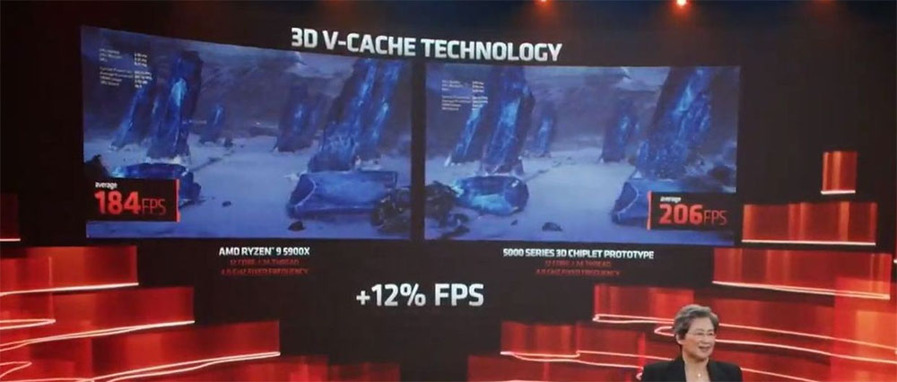
How does it benefit desktop users? It benefits us for gaming performance purposes because it supposes an increase in FPS in video games . Lisa Su showed a comparison between a Ryzen 9 5900X and a Zen 3- based prototype with a 3D chiplet design .
Both ran at 4.0 GHz and with the same GPU (not specified), and the truth is that the Ryzen 9 5900X achieved 184 FPS , while the chip with 3D V-Cache design achieved 206 FPS under the same conditions, why what? Well, the Ryzen 9 comes with 64MB L3, while the prototype equips 192MB L3, triple the cache!
They tried more games, but here they just gave us a performance multiplier as a figure:
- DOTA 2: 1.18x more.
- Gears V: 1.12x more.
- Monster Hunter World: 1.25x more.
- LoL: 1.04x more.
- Fortnite: 1.17x more.

We are talking about really good numbers without equipping more cores or a different manufacturing process, so it is clear that it is the next-gen innovation par excellence at AMD. This ensures that it offers 15% higher gaming performance , although you already know what to do with this data: take it with tweezers.
Finally, the question is whether there will be problems with cache latency , but AMD has confirmed that it will not have them because it has a strip of addresses as if it were an ordinary L3.
When will we see 3D V-Cache on Ryzen?
Starting with Ryzen 7000 based on Zen 4 , which would come with the novelties of DDR5 RAM support , as well as a 5nm manufacturing process. The production of these chips will be in charge of TSMC, since it is the favorite of AMD and who can produce chips with 3D stacking.
We hope this information has been helpful to you. If you have any questions, you can comment below and we will answer you as soon as possible.