HBM memory: what is this memory for GPU and CPU
Graphics cards make use of VRAM memory chips to store information that they need to access on a recurring basis. One of the types of memory that exist for graphics cards is High Brandwidth Memory (HBM), which has some advantages over other types of memory. HBM memory
Index of contents
What is HBM memory
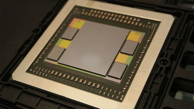
They are a type of high-speed computer memory that is characterized by offering dynamic random access synchronously with 3D stacking . HBM is a type of memory developed and mainly used for high-performance graphics accelerators, network devices, ASICs and FPGAs for AI for high-performance data centers, in supercomputers and in some models of gaming graphics cards.
The first HBM memory chip was manufactured by SK Hynix in 2013. The first serial products to integrate HBM memories were the AMD Fuji GPUs released in 2015.
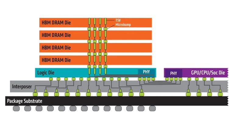
What HBM offers is high bandwidth with lower power consumption than DDR and GDDR standards. This is accomplished by stacking up to eight DRAM arrays and an optional base array that can include a buffer and test logic circuit. The stacked memories are vertically interconnected by through silicon pathways (TSV) and micro-welds (microbumps) . HBM memories are usually installed on the same substrate as the GPU and CPU.
AMD and NVIDIA use different variants of HBM memory embedded in the same package of the professional GPUs. HBM memories can also be integrated into the same CPU package. NVIDIA and AMD use special designs for these GPUs that integrate an interposer that makes HBM memories can be installed next to the GPU and thus obtain better performance and less consumption . The problem is that the manufacture of HBM memories is expensive and the GPUs that integrate them are also more expensive, since they require additional elements.
Development of HBM reports
This type of memory began to be developed in 2008 and it was AMD who began its development. What the company wanted was to create memories that would correct the problem of consumption and the form factor . The aim was to achieve a solution that would satisfy the increasing needs of the amount of memory of a computer, but occupying less space and consuming less.
AMD in the following years was working on the development of different procedures for stacking matrices . The team in charge of the development of these memories was Bryan Black, a senior member of AMD. Note that AMD sought the collaboration of industry partners with experience in memory manufacturing and development. One of the most prominent was SK Hynix, who already had prior experience building stacked memories in 3D. It also had the Taiwanese UMC , specialized in interposers, and Amkor Technology and ASE, two companies specialized in the encapsulation process.
HBM was completed in 2013, the year SK Hynix manufactured the first memory chip. JEDEC adopted HBM memories as standard in October 2013 , as a result of a request made by AMD and SK Hynix in 2010. Mass manufacturing of HBM memories by SK Hynix started in 2015.
The first commercial product to use HBM memory was AMD Fiji GPUs, which were launched in June 2015, with the AMD Radeon R9 Fury graphics card using them.
Samsung in January 2016 started the early manufacturing of the HBM2 memories . That same month, JEDEC accepted the HBM2 reports as a standard. The first commercial solution to use HBM2 memory was the NVIDIA Tesla P100 graphics card , which began shipping in April 2016. Intel shortly after, in June 2016, launched the Xeon Phi accelerators that feature 8 HCDRAM memory stacks, a variant of the HBM memories manufactured by Micron.
HBM memory features
These memories stand out as an especially exceptional solution for memory-intensive computing tasks. The main characteristics of these reports are:
Eliminate the processing bottleneck
The HBM memories have the characteristic of being able to be installed directly in the GPU / CPU package . What this allows is to reduce the distance that the information must travel, thanks to the interposer. Thus they connect to the GPU / CPU through high-performance and efficient pathways. While they are not physically integrated into the GPU / CPU, the transfer speed is incredible.
Energy efficiency
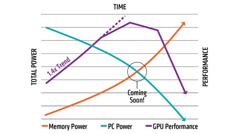
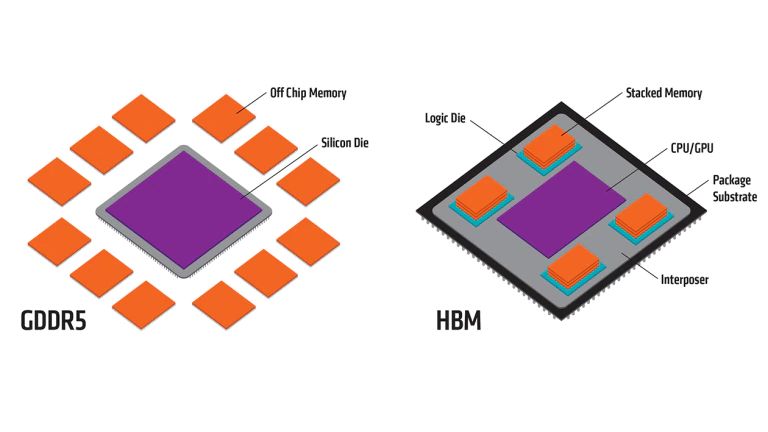
Opting for HBM memories is what it allows is to improve the energy efficiency of the system. Fewer memory chips are required per GPU , which at first reduces energy consumption compared to GDDR memory. But it is also that the HBM memories are next to the GPU , in the same package, while the GDDR memories are around the package of the GPU, which also significantly reduces power consumption.
Small form factor
Additionally, HBM memories are characterized by having a space-saving design. For the same amount of memory on a graphics card, HBM memories occupy up to 94% less than GDDR5 memories. Not only this, since HBM memories are integrated into the GPU package, the size of the PCB can be reduced with respect to GDDR memories.
Bandwidth
HBM memories offer a much higher bandwidth than that offered by GDDR memories. This makes HBM memories especially optimal for tasks such as Artificial Intelligence, Deep Learning, supercomputing and other situations where there is a huge flow of data.
Manufacturing costs
Not everything is lights with HBM memories, there is also a shadow and it is the manufacturing cost. The cost of manufacturing HBM memory wafers is estimated to be 30-50% more than a DRAM memory wafer (GDDR). This is due to the characteristics and manufacturing peculiarities of these memories. For this same reason, this type of memory is not used in gaming graphics cards, since it would greatly increase the final price.
HBM memory types
We are now going to do a little review of the different variants of HBM memories that have been appearing. Some of the reports that appear here are not yet commercialized, as they are still in the development phase.
Memories HBM
HBM memories offer a larger memory bus than other DRAM standards (such as DDR4 and GDDR5). An HBM stack makes use of four DRAM arrays (4-Hi) which has two 128-bit channels per array for a total of 8 channels and a 1024-bit memory interface (128GB / s bandwidth). Each of the memory stacks can have a maximum capacity of 4GB and up to 16GB of HBM memory can be installed .
A GPU with four 4-Hi HBM stacks can offer 4096-bit memory bandwidth. GDDR5 memory only offers 32 bits per channel and a maximum of 16 channels, thus offering a 512-bit memory interface.
Memories HBM2
It is the evolution of HBM memories, with significant performance and capacity improvements. The HBM2 memories are characterized by offering a bandwidth of 2656GB / s per stack and a limit of 8GB of memory per stack. They are also characterized by offering the possibility of integrating up to 8 memory stacks, offering a total capacity of 64GB HBM2.
Memories HBM2e
We could say that these memories are a “simple” update of the HBM2 memories. These new HBM2e memories are characterized by offering a bandwidth of up to 307GB / s per memory stack. This update allows the stacking of up to twelve layers of memory (12-Hi) allowing a total of 24GB per stack.
HBM2e has received two variants:
- Samsung: It has developed the HBM2 memories that have been called Flashbolt HBM2e and which has eight matrices per memory stack. These memories offer a capacity of 16GB and a bandwidth of 460GB / s per memory stack
- SK Hynix: You have developed a variant of the HBM2e memories that you have not renamed. This revision offers a capacity of 16GB and a bandwidth of up to 460GB / s.
Memories HBM3
By the end of 2020, the update to HBM2e was announced by Micron, which initially received the name of HBMnext memories. These memories have subsequently been renamed HBM3 memories . These new memories will offer a bandwidth per memory stack of 665GB / s . Each of the memory stacks can support up to 64GB of capacity in a 16-matrix (16-Hi) format. Additionally, these memories have licensed to Xperi Corp the hybrid interconnection technology DBI Ultra 2.5D / 3D.
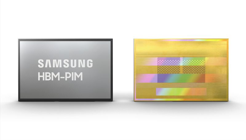
Memories HBM-PIM
Samsung in February 2021 announced the development of “special” HBM memories with memory processing. These memories have been developed entirely for AI computing within memory . This enables large-scale data processing capacity to be increased. It allows a DRAM-optimized AI engine to be installed within each memory stack that enables parallel processing and minimizes data movement. According to Samsung, the performance of the system will double and in addition, energy consumption will be reduced by 70%, without the need to change hardware or software.
Final words on the HBM memoirs
High Brandwith Memory memories have become essential for such important segments as artificial intelligence, deep learning and supercomputing, among others. HBM is a memory standard that has been adopted for graphics cards intended for advanced computing, such as those mentioned and is also being integrated into CPUs, what’s more, Intel Xeon Sapphire Rapids CPUs, which will be launched in 2022, some models will integrate memories HBM2e.
We recommend this article with the comparison of HBM2 memories and GDDR6 memories
AMD was the one who began its development to improve energy efficiency and that memory sizes could be scaled. But another reason is that the GCN architecture had a problem and that is that it required a large bandwidth or at least, the higher bandwidth with the memories, the better performance was obtained. This has been left behind with the RDNA architecture for gaming and the CDNA architecture for advanced computer graphics.
We see that HBM memories have evolved very well, but it is difficult for them to end up being used in the gaming market. The problem with HBM memories is that they are more difficult and expensive to manufacture than GDDR DRAM memories. We saw how the HBM2 memories assumed that the AMD Radeon Vega 64 were excessively expensive with respect to the performance they offered. While many suggest that HBM memories will end up replacing GDDR memories, at the moment this seems quite unfeasible economically.


